IMPORTANT NOTE: I have mentioned this already in the previous tutorials but I will repeat it in every LPC1768 Tutorial. Download both the Datasheet and User Manual for LPC1768 MCU from the official NXP website. I cannot explain / discuss each and every topic in detail. You have to look up for the topic of discussion in those documents and gather additional information.
Introduction
DAC is short for Digital to Analog Converter. It is quite opposite to an ADC (Analog to Digital Converter) and it is one of the simplest and easy to use peripherals of an Arm Cortex-M3 MCU. Primarily DACs are used in audio equipment like Music Players to convert the digital data into analog audio signals. Similarly, there are video DACs, for converting digital video data into analog video signals to be displayed on a screen. There are different types of DAC implementations like Switched Resistor DAC, R – 2R Ladder DAC, Successive Approximation DAC, etc. One of the simplest ways to implement a DAC is to using the PWM Functionality of a Timer Peripheral (if dedicated DAC unit is nor present). Similar to an ADC, a DAC also has resolution. It indicated the number of possible values a DAC unit can produce between the voltage extremes. For example, an 8-bit DAC can produce 28 i.e. 256 different levels for a voltage range.
DAC in LPC1768 MCU
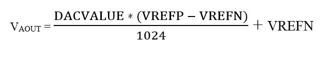
Coming to the DAC in LPC1768 MCU, it contains a 10-bit DAC peripheral based on Resistor String Architecture. It can produce buffered output and the maximum update rate is 1 MHz. Since the resolution of the DAC in LPC1768 is 10-bit, it can produce 210 different values between the positive and the negative reference voltage levels. The output voltage of a DAC can be calculated using the following formula.
Where,
VAOUT = Output Analog Voltage of DAC VREFP = Positive Reference Voltage of DAC VREFN = Negative Reference Voltage of DAC DACVALUE = 10-bit digital value, which must be converted to analog voltage.
Pins Associated with DAC
Since there is only a single channel in the DAC, only one output pin of the DAC Peripheral. The remaining pins related to power. Following table gives an overview of pins associated with DAC peripheral of LPC1768 MCU. Pin Function Description AOUT – P0.26 Analog Output Provides the analog output voltage with reference to the analog GND (VSSA). VREFP, VREFN Voltage References These pins provide the positive and negative reference voltages for DAC and ADC. Usually isolated 3.3V and 0V. VDDA, VSSA Analog Power and GND Same as VDD and VSS but isolated to minimize noise.
LPC1768 DAC Registers
Let us now see the registers associated with DAC of LPC1768. There are totally three registers for DAC in LPC1768. They are DACR, DACCTRL and DACCNTVAL. The DACCTRL and DACCNTVAL registers are associated with DMA operations in DAC. So, let us focus on the DACR i.e. the D/A Converter Register. DACR – D/A Converter Register: It contains the digital value that must be converted to analog value. Also, this register contains a bit for a trade-off between power and performance. Bits [15:6] VALUE These bits contain the digital value (DACVALUE) that is to be converted to analog value (VAOUT) based on the previously mentioned formula. Bit [16] BIAS When 0, settling time of DAC is 1 µS (update rate is 1 MHz), max current is 700 µA. When 1, settling time of DAC is 2.5 µS (update rate is 400 kHz), max current is 350 µA.
Example
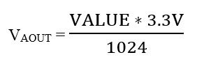
Let us now see a simple example program for using DAC in LPC1768 MCU. If DMA operations is not used, then programming DAC peripheral is very simple. Just configure P.026 pin as AOUT and load the 10-bit digital value in the DACR register. You will get the converted analog value as the output. When 1, settling time of DAC is 2.5 µS (update rate is 400 kHz), max current is 350 µA. There is no power control pin for DAC in LPC1768, in contrast to most of the other peripherals. In order to enable the DAC Peripheral, all you have to do is configure the relevant pin as DACOUT i.e. make P0.26 as AOUT. Another important property of DAC is its reference voltages. Usually, the VREFP is connected to 3.3V (isolated from main VDD) and the VREFN is connected to 0V (also isolated from main VSS). If we use the above reference voltage values, then the output of the DAC at AOUT pin can be calculated using the following formula:
So, by simply writing a 10-bit value i.e. between 0 and 1023 in the VALUE bits of DACR register, you can get an analog voltage between 0V and 3.3V. Another important factor of DAC is the trade-off between power and performance. In this example, we will be using the smallest possible settling time i.e. 1 µS by setting the BIAS bit in DACR register as 0. This means that the update frequency of the DAC output is 1 MHz.
Code
#include <lpc17xx.h> void Timer0_Init(void); void delayms(unsigned int milliseconds); int main(void) { Timer0_Init(); LPC_PINCON->PINSEL1 |= (1«21); unsigned int value=0; while(1) { if(value > 1023) { value=0; } LPC_DAC->DACR = (value«6); delayms(10); value++; } } void Timer0_Init(void) { LPC_TIM0->CTCR = 0x0; LPC_TIM0->PR = 25000-1; LPC_TIM0->TCR = 0x02; } void delayms(unsigned int milliseconds) { LPC_TIM0->TCR = 0x02; LPC_TIM0->TCR = 0x01; while(LPC_TIM0->TC < milliseconds); LPC_TIM0->TCR = 0x00; } I have used Timer0 peripheral to generate the desired delay. So, check out my LPC1768 Timer Tutorial.
Conclusion
A simple tutorial on how to use DAC in LPC1768 MCU is explained here. Using the DAC Peripheral, you can generate different analog waveforms like square wave, sinusoidal wave, saw-tooth wave etc. Comment * Name * Email * Website
Δ
![]()
![]()
![]()
![]()
![]()

