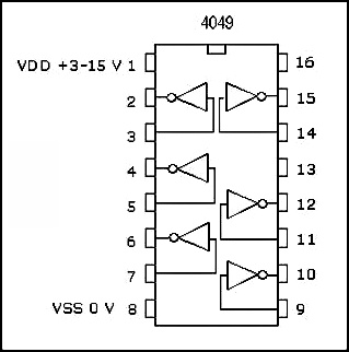
As shown in the above figure, CD4049 holds six inverter gates on a single package. In this IC, for input purpose pin 3 is used while for the output purpose, pin 2 is used for the first gate. In the same way for the second gate, pin 5 is used as input and pin 4 as an output terminal and in the same manner for rest all the gates. For the supply voltage pin 1 is used and for the ground purpose pin 8 is used. While pin number 13 and 16 are not used. The IC works on the voltage range from 3V to 15V excessive voltage more than 15V will destroy the IC. So provide input voltage in the range of 3V to 15V.
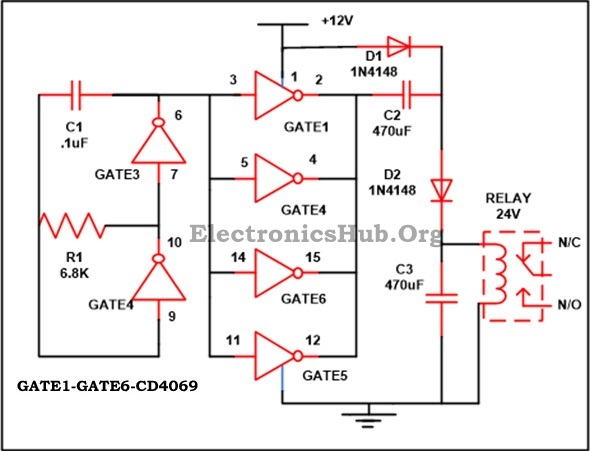
Circuit Diagram of 12V to 24V DC Converter:
Circuit Components:
IC CD4049 – 1 Resistor R1(6.8K) – 1 C1(.1uF) – 1 C2,C3(470uF) – 2 D1,D2(1N4148) – 2 RELAY – 1
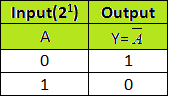
Description: In this circuit for doubling the input voltage, we are using NOT gate CD4049 IC. In this circuit, we are using all 6 gates of NOT gate. Before getting familiar with the working of the circuit it is important that one should get familiar with the NOT gate truth table which is as follows-
In the NOT, if we supply logic low (i.e. 0) In the input terminal then we receive logic high (i.e. 1) at the output terminal. Similarly, if we give logic high (i.e. 1) at the input terminal then we receive logic low (i.e. 0) at the output terminal. As describe above CD4049 holds six inverter gates on a single package. In this IC for input is given to pin 3 is while output is taken from pin 2 from the first gate. In the same way for the second gate pin 5 is used as input and pin 4 as an output terminal and in the same manner for rest all the gates. Connect pin 1 to power supply and pin 8 to ground. Assemble the circuit properly and now provide power supply. In this circuit we are utilizing all six gates of the NOT gate. With the assist of the pin 3 and pin 4 we have firstly construct an oscillator along with capacitor C1 as well as resistor R1.With the help of value of R1 and C1 the oscillation frequency is calculated. The reset left gates are connected to the parallel to work like a buffer. All the input pin i.e. 3, 5, 11 and 14 are linked together and connected with the frequency source through oscillator. In the same way all the output pins, i.e. 2,4,12 and 15 are linked together and connected to the voltage enhance circuit. By the support of the capacitor as well as resistor a voltage multiplier circuit can be constructed. This circuit is mainly used at the time when we need to produce more output voltage as compared with the given input voltage. In this circuit, we are using largely accepted generally employed half wave series multiplier. For the construction of the voltage doubler circuit, we have a requirement of 2 diodes, 2 capacitors along with an oscillating voltage.As you can find in the circuit diagram that the diode D1 works in the forward bias state and which in turn charge the capacitor C2 till it reaches to the peak value of input voltage supply which is now rotate like a battery in series along the power supply. At the similar period of time diode D2 starts conducting due to diode D1 and capacitor C3 charges. Hence the voltage that we receive at the C3 is the total voltage of the voltage supply and the voltage across capacitor C2. The chief advantage of this circuit is that it permits to produce higher value of voltage from a very low value of input source voltage and there is no need to use a transformer in the circuit. So at the output terminal of the diode D2 you can run 24V relay with the assist of 12V of power supply. Comment * Name * Email * Website
Δ
![]()
![]()
![]()
![]()
![]()

